- 您现在的位置:买卖IC网 > Sheet目录491 > NTMFS4934NT1G (ON Semiconductor)MOSFET N-CH 30V 147A SO8 FL
�� �
�
�NTMFS4934N�
�Power� MOSFET�
�30� V,� 147� A,� Single� N� ?� Channel,� SO� ?� 8� FL�
�Features�
�?� Low� R� DS(on)� to� Minimize� Conduction� Losses�
�?� Low� Capacitance� to� Minimize� Driver� Losses�
�?� Optimized� Gate� Charge� to� Minimize� Switching� Losses�
�?� These� Devices� are� Pb� ?� Free,� Halogen� Free/BFR� Free� and� are� RoHS�
�Compliant�
�Applications�
�?� CPU� Power� Delivery,� DC� ?� DC� Converters�
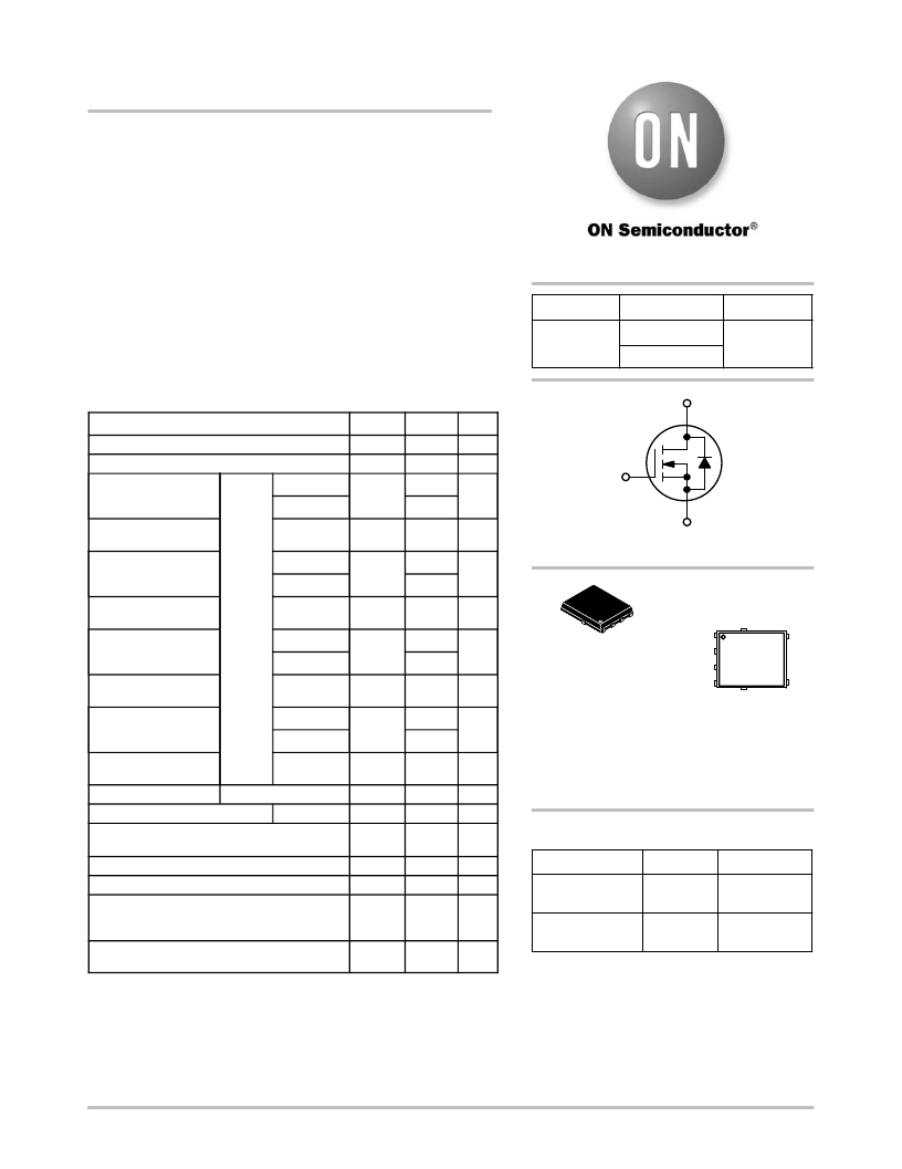
�MAXIMUM� RATINGS� (T� J� =� 25� °� C� unless� otherwise� stated)�
�V� (BR)DSS�
�30� V�
�http://onsemi.com�
�R� DS(ON)� MAX�
�2.0� m� W� @� 10� V�
�3.0� m� W� @� 4.5� V�
�D� (5,6)�
�I� D� MAX�
�147� A�
�Parameter�
�Drain� ?� to� ?� Source� Voltage�
�Symbol�
�V� DSS�
�Value�
�30�
�Unit�
�V�
�Gate� ?� to� ?� Source� Voltage�
�Continuous� Drain�
�Current� R� q� JA�
�(Note� 1)�
�Power� Dissipation�
�R� q� JA� (Note� 1)�
�T� A� =� 25� °� C�
�T� A� =� 100� °� C�
�T� A� =� 25� °� C�
�V� GS�
�I� D�
�P� D�
�±� 20�
�29.1�
�18.4�
�2.72�
�V�
�A�
�W�
�G� (4)�
�S� (1,2,3)�
�N� ?� CHANNEL� MOSFET�
�Continuous� Drain�
�Current� R� q� JA� ≤� 10� s�
�(Note� 1)�
�Power� Dissipation�
�R� q� JA� ≤� 10� s� (Note� 1)�
�Continuous� Drain�
�Current� R� q� JA�
�(Note� 2)�
�Power� Dissipation�
�R� q� JA� (Note� 2)�
�Steady�
�State�
�T� A� =� 25� °� C�
�T� A� =� 100� °� C�
�T� A� =� 25� °� C�
�T� A� =� 25� °� C�
�T� A� =� 100� °� C�
�T� A� =� 25� °� C�
�I� D�
�P� D�
�I� D�
�P� D�
�47.5�
�30.0�
�7.23�
�17.1�
�10.8�
�0.93�
�A�
�W�
�A�
�W�
�1�
�SO� ?� 8� FLAT� LEAD�
�CASE� 488AA�
�STYLE� 1�
�S�
�S�
�S�
�G�
�MARKING�
�DIAGRAM�
�D�
�4934N�
�AYWZZ�
�D�
�D�
�D�
�Continuous� Drain�
�Current� R� q� JC�
�(Note� 1)�
�Power� Dissipation�
�R� q� JC� (Note� 1)�
�Pulsed� Drain� Current�
�T� C� =� 25� °� C�
�T� C� =100� °� C�
�T� C� =� 25� °� C�
�T� A� =� 25� °� C,� t� p� =� 10� m� s�
�I� D�
�P� D�
�I� DM�
�147�
�93�
�69.44�
�442�
�A�
�W�
�A�
�A�
�Y�
�W�
�ZZ�
�=� Assembly� Location�
�=� Year�
�=� Work� Week�
�=� Lot� Traceability�
�Current� Limited� by� Package�
�T� A� =� 25� °� C�
�I� Dmax�
�100�
�A�
�Operating� Junction� and� Storage� Temperature�
�T� J� ,�
�T� STG�
�?� 55� to�
�+150�
�°� C�
�ORDERING� INFORMATION�
�Source� Current� (Body� Diode)�
�I� S�
�68�
�A�
�Device�
�Package�
�Shipping� ?�
�Drain� to� Source� DV/DT� dV/d� t� 6� V/ns�
�Single� Pulse� Drain� ?� to� ?� Source� Avalanche� E� AS� 205� mJ�
�Energy� T� J� =� 25� °� C,� V� DD� =� 24� V,� V� GS� =� 10� V,�
�I� L� =� 37� A� pk� ,� L� =� 0.3� mH,� R� G� =� 25� W�
�Lead� Temperature� for� Soldering� Purposes� T� L� 260� °� C�
�(1/8� ″� from� case� for� 10� s)�
�Stresses� exceeding� Maximum� Ratings� may� damage� the� device.� Maximum�
�Ratings� are� stress� ratings� only.� Functional� operation� above� the� Recommended�
�Operating� Conditions� is� not� implied.� Extended� exposure� to� stresses� above� the�
�Recommended� Operating� Conditions� may� affect� device� reliability.�
�1.� Surface� ?� mounted� on� FR4� board� using� 1� sq� ?� in� pad,� 1� oz� Cu.�
�2.� Surface� ?� mounted� on� FR4� board� using� the� minimum� recommended� pad� size.�
�NTMFS4934NT1G� SO� ?� 8� FL� 1500� /�
�(Pb� ?� Free)� Tape� &� Reel�
�NTMFS4934NT3G� SO� ?� 8� FL� 5000� /�
�(Pb� ?� Free)� Tape� &� Reel�
�?For� information� on� tape� and� reel� specifications,�
�including� part� orientation� and� tape� sizes,� please�
�refer� to� our� Tape� and� Reel� Packaging� Specifications�
�Brochure,� BRD8011/D.�
�?� Semiconductor� Components� Industries,� LLC,� 2012�
�May,� 2012� ?� Rev.� 4�
�1�
�Publication� Order� Number:�
�NTMFS4934N/D�
�发布紧急采购,3分钟左右您将得到回复。
相关PDF资料
NTMFS4935NCT3G
MOSFET N-CH 30V SO8-FL
NTMFS4936NCT3G
MOSFET N-CH 30V 11.6A SO-8FL
NTMFS4937NT1G
MOSFET N-CH 30V 10.2A SO8 FL
NTMFS4939NT3G
MOSFET N-CH 30V 9.3A SO8 FL
NTMFS4941NT3G
MOSFET N-CH 30V 9A SO8 FL
NTMFS4943NT1G
MOSFET N-CH 30V 8.3A SO8 FL
NTMFS4945NT3G
MOSFET N-CH 30V 7.4A SO8 FL
NTMFS5830NLT1G
MOSFET N-CH 40V 28A SO-8FL
相关代理商/技术参数
NTMFS4934NT3G
功能描述:MOSFET Power MOSFET 30V 147A 2m OHM RoHS:否 制造商:STMicroelectronics 晶体管极性:N-Channel 汲极/源极击穿电压:650 V 闸/源击穿电压:25 V 漏极连续电流:130 A 电阻汲极/源极 RDS(导通):0.014 Ohms 配置:Single 最大工作温度: 安装风格:Through Hole 封装 / 箱体:Max247 封装:Tube
NTMFS4935N
制造商:ONSEMI 制造商全称:ON Semiconductor 功能描述:Power MOSFET 30 V, 93 A, Single N−Channel, SO−8 FL
NTMFS4935NBT1G
功能描述:MOSFET NFET SO8FL 30V 93A 3.2 mOhm RoHS:否 制造商:STMicroelectronics 晶体管极性:N-Channel 汲极/源极击穿电压:650 V 闸/源击穿电压:25 V 漏极连续电流:130 A 电阻汲极/源极 RDS(导通):0.014 Ohms 配置:Single 最大工作温度: 安装风格:Through Hole 封装 / 箱体:Max247 封装:Tube
NTMFS4935NBT3G
功能描述:MOSFET NFET SO8FL 30V 93A 3.2 mOhm RoHS:否 制造商:STMicroelectronics 晶体管极性:N-Channel 汲极/源极击穿电压:650 V 闸/源击穿电压:25 V 漏极连续电流:130 A 电阻汲极/源极 RDS(导通):0.014 Ohms 配置:Single 最大工作温度: 安装风格:Through Hole 封装 / 箱体:Max247 封装:Tube
NTMFS4935NCT1G
功能描述:MOSFET TRENCH 3 S08FL, 30V NCH M RoHS:否 制造商:STMicroelectronics 晶体管极性:N-Channel 汲极/源极击穿电压:650 V 闸/源击穿电压:25 V 漏极连续电流:130 A 电阻汲极/源极 RDS(导通):0.014 Ohms 配置:Single 最大工作温度: 安装风格:Through Hole 封装 / 箱体:Max247 封装:Tube
NTMFS4935NCT3G
功能描述:MOSFET N-CH 30V SO8-FL RoHS:是 类别:分离式半导体产品 >> FET - 单 系列:- 标准包装:1,000 系列:MESH OVERLAY™ FET 型:MOSFET N 通道,金属氧化物 FET 特点:逻辑电平门 漏极至源极电压(Vdss):200V 电流 - 连续漏极(Id) @ 25° C:18A 开态Rds(最大)@ Id, Vgs @ 25° C:180 毫欧 @ 9A,10V Id 时的 Vgs(th)(最大):4V @ 250µA 闸电荷(Qg) @ Vgs:72nC @ 10V 输入电容 (Ciss) @ Vds:1560pF @ 25V 功率 - 最大:40W 安装类型:通孔 封装/外壳:TO-220-3 整包 供应商设备封装:TO-220FP 包装:管件
NTMFS4935NT1G
功能描述:MOSFET NFET SO8FL 30V RoHS:否 制造商:STMicroelectronics 晶体管极性:N-Channel 汲极/源极击穿电压:650 V 闸/源击穿电压:25 V 漏极连续电流:130 A 电阻汲极/源极 RDS(导通):0.014 Ohms 配置:Single 最大工作温度: 安装风格:Through Hole 封装 / 箱体:Max247 封装:Tube
NTMFS4935NT3G
功能描述:MOSFET NFET SO8FL 30V RoHS:否 制造商:STMicroelectronics 晶体管极性:N-Channel 汲极/源极击穿电压:650 V 闸/源击穿电压:25 V 漏极连续电流:130 A 电阻汲极/源极 RDS(导通):0.014 Ohms 配置:Single 最大工作温度: 安装风格:Through Hole 封装 / 箱体:Max247 封装:Tube